Technology
Chinese Internet Authority Clashes with Google Over Digital Certificates
(PC World) – A Chinese Internet administrator blasted Google on Thursday, after the U.S. search giant decided to stop recognizing digital certificates issued by the group following a security lapse.
“The decision that Google has made is unacceptable and unintelligible,” China’s Internet Network Information Center (CNNIC) said in an online posting.
Google’s decision means that its Chrome browser could end up clashing with sites served by the Chinese Internet agency.
On Wednesday, Google explained the move in an update to an earlier blog posting. The company is still concerned by the way CNNIC issued a certificate to an IT company based in Egypt that misused it in a botched security test.
Alameda County
OPINION: Argent Materials Oakland CleanTech Community Asset Helps Those In Need
Alameda County Supervisor Lena Tam had this to say about Argent Materials as an Oakland community asset: “Congratulations to Argent Materials and its President and Founder, Bill Crotinger! The company is now fully operational, recycling an impressive 99.99% of concrete and asphalt debris, which helps divert thousands of tons of construction waste from landfills. They are also proud to announce that 50% of their team consists of local hires. In celebration of Thanksgiving, and despite stormy weather last week, the Alameda County Sheriffs, alongside Mr. Crotinger and Argent Materials’ dedicated staff distributed turkeys and pies as a heartfelt gesture of gratitude to the community.”

Zennie Abraham
CEO, Zennie62Media
Argent Materials, the Oakland business that turns old concrete and asphalt into new construction products, generally goes by “Argent Materials Oakland CleanTech” but should be called “Argent Materials East Oakland CleanTech for The Community”. Here’s why.
First, Argent Materials is located at 8300 Baldwin St, right in the Coliseum Industrial Zone, just a three-minute drive from the Oakland-Alameda County Coliseum Complex. That’s in East Oakland, and just a city-block walk from the Oakland Coliseum BART Station.
Second, Argent Materials has been a friend to East Oakland and what some, like the members of the Oakland Private Industry Council, would call a “community asset”. In 2024, Argent Materials founder and President Bill Crotinger was named Leader of the Year by the Oakland Private Industry Council (OPIC) “I was humbled and honored to be named Leader of the Year by the Oakland Private Industry Council. Truly an honor. My heartfelt thanks to my friend and mentor Pastor Raymond Lankford and all the wonderful people at OPIC.”
Alameda County Supervisor Lena Tam had this to say about Argent Materials as an Oakland community asset: “Congratulations to Argent Materials and its President and Founder, Bill Crotinger! The company is now fully operational, recycling an impressive 99.99% of concrete and asphalt debris, which helps divert thousands of tons of construction waste from landfills. They are also proud to announce that 50% of their team consists of local hires. In celebration of Thanksgiving, and despite stormy weather last week, the Alameda County Sheriffs, alongside Mr. Crotinger and Argent Materials’ dedicated staff distributed turkeys and pies as a heartfelt gesture of gratitude to the community.”
ABI Foundry reports that Argent Materials led a community clean up for the residents and businesses of Russett Street as well as San Leandro Street. An ABI Foundry team member said “Bill Crotinger at Argent Materials spearheaded the initiative to clean San Leandro street, from Hegenburger to 98th Ave. along the side of BART. AB&I enjoyed participating along with Acts Full Gospel C.O.G.I.C (Men of Valor), Good Hope Missionary Baptist Church-Oakland (Reverend Michael Jones) and Argent Materials. You should see how it looks now. It is AMAZING! It takes an ambitious mind to make a difference block by block.”
What Is Cleantech And Why Is It Important to Oakland And Argent Materials?
Clean technology (Clean Tech) refers to products, services, and processes that mitigate negative environmental impacts by increasing energy efficiency, promoting resource sustainability, and minimizing waste and pollution, ultimately contributing to a low-carbon, and more sustainable economy.
What is The Clean Tech of Argent Materials of Oakland?
In Argent Materials’ context, “cleantech” refers to their sustainable business model which includes recycling concrete and asphalt into new aggregate materials, diverting waste from landfills, and using renewable diesel for their fleet to achieve carbon neutrality and protect the environment. This business approach Argent Materials uses aligns with the broader definition of cleantech, which involves products, services, and processes that reduce negative environmental impacts through resource efficiency and environmental protection
Clean Tech, or green tech as Argent Materials of Oakland does it, is defined as any technology that minimizes negative environmental impact by reducing human consumption of natural resources and by promoting more sustainable and efficient resource use.
Argent Materials will continue to be a cleantech community asset to Oakland well into the future.
Stay tuned.
Activism
Golden State Warriors Program Is Inspiring Next Generation of Female Engineers
Breaking down barriers and biases that deter young girls from pursuing STEAM subjects is essential for creating a level playing field and ensuring equal opportunities for all. By challenging stereotypes and promoting a culture of inclusivity and diversity in STEAM fields, experts believe young girls can be empowered to pursue their interests and aspirations without limitations confidently. Encouraging mentorship, providing access to resources, and celebrating girls’ achievements in STEAM are all crucial steps in creating a supportive environment that fosters success.

By Y’Anad Burrell
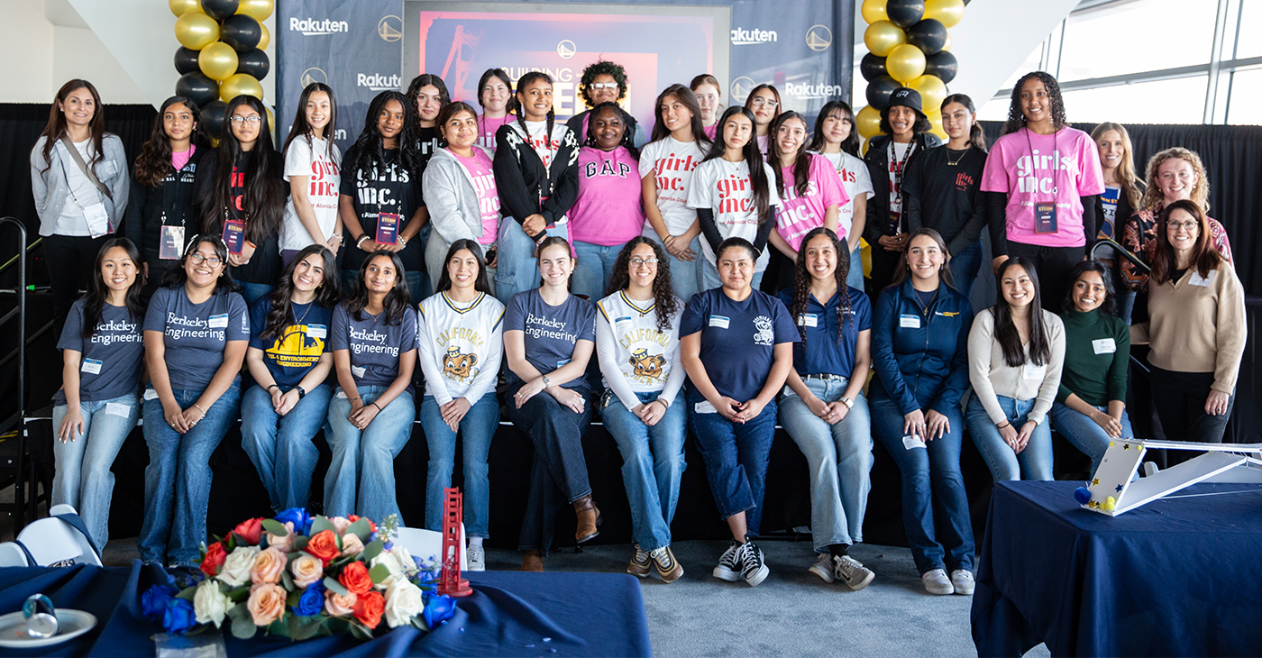
The Golden State Warriors and e-commerce giant Rakuten are joining forces to inspire the next generation of female engineers through Building STEAM Futures, part of The City Calls campaign.
Organizers say the initiative is founded on the idea that science, technology, engineering, arts, and mathematics (STEAM) are crucial fields for innovation and progress, and empowering young girls to pursue careers in these areas is more important than ever. Studies consistently show that girls are underrepresented in STEAM fields, resulting in a gender disparity that limits potential and hinders diversity.
Breaking down barriers and biases that deter young girls from pursuing STEAM subjects is essential for creating a level playing field and ensuring equal opportunities for all. By challenging stereotypes and promoting a culture of inclusivity and diversity in STEAM fields, experts believe young girls can be empowered to pursue their interests and aspirations without limitations confidently. Encouraging mentorship, providing access to resources, and celebrating girls’ achievements in STEAM are all crucial steps in creating a supportive environment that fosters success.
On Saturday, March 8, International Women’s Day, the Warriors and Rakuten hosted 20 middle school girls from Girls Inc. of Alameda County at Chase Center’s Above the Rim for a hands-on bridge-building experience. The young girls from Girls, Inc. of Alameda County had an opportunity to design, build and test their own bridge prototypes and learn the fundamentals of bridge construction from the Engineering Alliance and the UC Berkeley Steel Bridge Team.
This STEAM experience for the girls followed the first session in January, where they took a behind-the-scenes tour of the Golden Gate Bridge, learning about its design and construction from industry experts. The City Calls campaign, tipped off with the unveiling the Warriors’ new bridge-themed City Edition jerseys and court design earlier this year.
Activism
Self-eSTEM Empowers BIPOC Women, Girls in Science, Math
In January 2025, Self-eSTEM will launch digital and generative AI programming, which provides digital literacy and AI literacy training through an entrepreneurial project-based activity. This programming will be a hybrid (i.e. in-person and online). Additionally, thanks to a grant from Comcast, in spring 2025, the organization will have a co-ed series for middle and high school students.

By Y’Anad Burrell
Special to The Post
In a world where technology plays an increasingly central role in all aspects of life, the importance of Science, Technology, Engineering, and Math (STEM) education cannot be overstated. Recognizing the significance of STEM for the future, focusing on young women and girls is a critical step in achieving gender equality and empowering the next generation.
Self-eSTEM, an Oakland-based non-profit organization, was founded by Adamaka Ajaelo, an Oakland native who had a successful corporate career with several Bay Area technology and non-tech companies. Ajaelo boldly decided to step away from these companies to give 100% of her time and talent to the non-profit organization she started in 2014 in the belief that she can change the game in innovation and future STEM leaders.
Over the course of a decade, Ajaelo has provided futurist tech programming to more than 2,000 BIPOC women and girls. The organization has an Early STEM Immersion Program for ages 7-17, Emerging Leaders Workshops for ages 18-25 and volunteer network opportunities for ages 25 and up.
In January 2025, Self-eSTEM will launch digital and generative AI programming, which provides digital literacy and AI literacy training through an entrepreneurial project-based activity. This programming will be a hybrid (i.e. in-person and online). Additionally, thanks to a grant from Comcast, in spring 2025, the organization will have a co-ed series for middle and high school students.
While the organization’s programs center on innovation and technology, participants also gain other valuable skills critical for self-development as they prepare for a workforce future. “Self-eSTEM encourages young women to expand on teamwork, communication, creativity, and problem-solving skills. The organization allows young women to enter STEM careers and pathways,” said Trinity Taylor, a seventh-year innovator.
“Our journey over the last decade is a testament to the power of community and opportunity, and I couldn’t be more excited for what the future holds as we continue to break barriers and spark dreams,” said Ajaelo.
“By encouraging girls to explore STEM fields from a young age, we foster their intellectual growth and equip them with the tools needed to thrive in a competitive global economy,” Ajaelo says.
Empowering young girls through STEM education is also a key driver of innovation and progress. When young women and girls are encouraged to pursue careers in STEM, they bring unique perspectives and problem-solving approaches to the table, leading to more diverse and inclusive solutions. This diversity is crucial for driving creativity and pushing boundaries in scientific and technological advancements.
Self-eSTEM has fundraising opportunities year-round, but year-end giving is one of the most critical times to support the program. Visit www.selfestem.org to donate to the organization, as your generosity and support will propel programming support for today’s innovators.
You will also find more details about Self-eSTEM’s programs on their website and social channels @selfestemorg
-

 Activism3 weeks ago
Oakland Post: Week of November 12 – 18, 2025
-

 Activism3 weeks ago
IN MEMORIAM: William ‘Bill’ Patterson, 94
-

 Activism3 weeks ago
How Charles R. Drew University Navigated More Than $20 Million in Fed Cuts – Still Prioritizing Students and Community Health
-

 Bay Area3 weeks ago
No Justice in the Justice System
-

 #NNPA BlackPress3 weeks ago
The Perfumed Hand of Hypocrisy: Trump Hosted Former Terror Suspect While America Condemns a Muslim Mayor
-

 #NNPA BlackPress2 weeks ago
Lewis Hamilton set to start LAST in Saturday Night’s Las Vegas Grand Prix
-

 #NNPA BlackPress2 weeks ago
Trump’s Death Threat Rhetoric Sends Nation into Crisis
-

 #NNPA BlackPress4 weeks ago
Protecting Pedophiles: The GOP’s Warped Crusade Against Its Own Lies


