Technology
Facebook Gives Users More Control Over Their News Feeds
(New York Times) – A perennial complaint from Facebook users is that they don’t have much control over what appears in their news feed, the main flow of posts on their Facebook home page or app screen. The social network’s mysterious computer algorithm analyzes thousands of signals, then spits out what it thinks you want to see based on the kinds of posts you have liked in the past and who you tend to interact with or ignore on the service.
On Thursday, Facebook announced a set of features that will give each person more control over what he or she wants to see. In essence, you get to reprogram the algorithm.
The most important new control allows you to tell Facebook that certain friends and pages — your spouse, your best friend, your child’s school, or hey, your favorite New York-based news organization — are so important to you that you want to see everything that they post. Facebook will then put those posts at the top of your feed.
“It’s really for the things you care about most,” said Adam Mosseri, the Facebook product management director who oversees the news feed. One of his colleagues, for example, loves Humans of New York and has put that page on his “see first” list.
Activism
Golden State Warriors Program Is Inspiring Next Generation of Female Engineers
Breaking down barriers and biases that deter young girls from pursuing STEAM subjects is essential for creating a level playing field and ensuring equal opportunities for all. By challenging stereotypes and promoting a culture of inclusivity and diversity in STEAM fields, experts believe young girls can be empowered to pursue their interests and aspirations without limitations confidently. Encouraging mentorship, providing access to resources, and celebrating girls’ achievements in STEAM are all crucial steps in creating a supportive environment that fosters success.

By Y’Anad Burrell
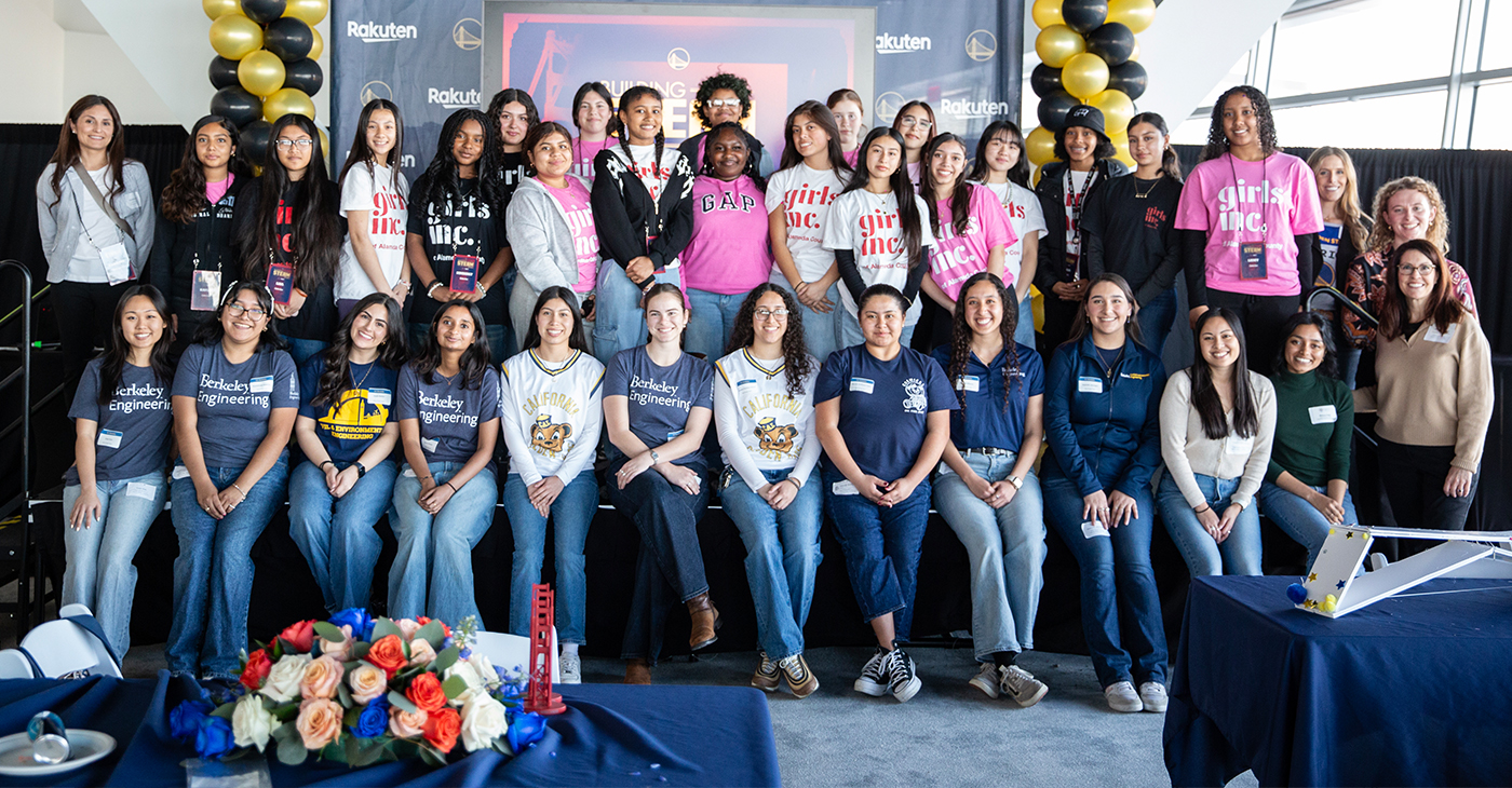
The Golden State Warriors and e-commerce giant Rakuten are joining forces to inspire the next generation of female engineers through Building STEAM Futures, part of The City Calls campaign.
Organizers say the initiative is founded on the idea that science, technology, engineering, arts, and mathematics (STEAM) are crucial fields for innovation and progress, and empowering young girls to pursue careers in these areas is more important than ever. Studies consistently show that girls are underrepresented in STEAM fields, resulting in a gender disparity that limits potential and hinders diversity.
Breaking down barriers and biases that deter young girls from pursuing STEAM subjects is essential for creating a level playing field and ensuring equal opportunities for all. By challenging stereotypes and promoting a culture of inclusivity and diversity in STEAM fields, experts believe young girls can be empowered to pursue their interests and aspirations without limitations confidently. Encouraging mentorship, providing access to resources, and celebrating girls’ achievements in STEAM are all crucial steps in creating a supportive environment that fosters success.
On Saturday, March 8, International Women’s Day, the Warriors and Rakuten hosted 20 middle school girls from Girls Inc. of Alameda County at Chase Center’s Above the Rim for a hands-on bridge-building experience. The young girls from Girls, Inc. of Alameda County had an opportunity to design, build and test their own bridge prototypes and learn the fundamentals of bridge construction from the Engineering Alliance and the UC Berkeley Steel Bridge Team.
This STEAM experience for the girls followed the first session in January, where they took a behind-the-scenes tour of the Golden Gate Bridge, learning about its design and construction from industry experts. The City Calls campaign, tipped off with the unveiling the Warriors’ new bridge-themed City Edition jerseys and court design earlier this year.
Activism
Self-eSTEM Empowers BIPOC Women, Girls in Science, Math
In January 2025, Self-eSTEM will launch digital and generative AI programming, which provides digital literacy and AI literacy training through an entrepreneurial project-based activity. This programming will be a hybrid (i.e. in-person and online). Additionally, thanks to a grant from Comcast, in spring 2025, the organization will have a co-ed series for middle and high school students.

By Y’Anad Burrell
Special to The Post
In a world where technology plays an increasingly central role in all aspects of life, the importance of Science, Technology, Engineering, and Math (STEM) education cannot be overstated. Recognizing the significance of STEM for the future, focusing on young women and girls is a critical step in achieving gender equality and empowering the next generation.
Self-eSTEM, an Oakland-based non-profit organization, was founded by Adamaka Ajaelo, an Oakland native who had a successful corporate career with several Bay Area technology and non-tech companies. Ajaelo boldly decided to step away from these companies to give 100% of her time and talent to the non-profit organization she started in 2014 in the belief that she can change the game in innovation and future STEM leaders.
Over the course of a decade, Ajaelo has provided futurist tech programming to more than 2,000 BIPOC women and girls. The organization has an Early STEM Immersion Program for ages 7-17, Emerging Leaders Workshops for ages 18-25 and volunteer network opportunities for ages 25 and up.
In January 2025, Self-eSTEM will launch digital and generative AI programming, which provides digital literacy and AI literacy training through an entrepreneurial project-based activity. This programming will be a hybrid (i.e. in-person and online). Additionally, thanks to a grant from Comcast, in spring 2025, the organization will have a co-ed series for middle and high school students.
While the organization’s programs center on innovation and technology, participants also gain other valuable skills critical for self-development as they prepare for a workforce future. “Self-eSTEM encourages young women to expand on teamwork, communication, creativity, and problem-solving skills. The organization allows young women to enter STEM careers and pathways,” said Trinity Taylor, a seventh-year innovator.
“Our journey over the last decade is a testament to the power of community and opportunity, and I couldn’t be more excited for what the future holds as we continue to break barriers and spark dreams,” said Ajaelo.
“By encouraging girls to explore STEM fields from a young age, we foster their intellectual growth and equip them with the tools needed to thrive in a competitive global economy,” Ajaelo says.
Empowering young girls through STEM education is also a key driver of innovation and progress. When young women and girls are encouraged to pursue careers in STEM, they bring unique perspectives and problem-solving approaches to the table, leading to more diverse and inclusive solutions. This diversity is crucial for driving creativity and pushing boundaries in scientific and technological advancements.
Self-eSTEM has fundraising opportunities year-round, but year-end giving is one of the most critical times to support the program. Visit www.selfestem.org to donate to the organization, as your generosity and support will propel programming support for today’s innovators.
You will also find more details about Self-eSTEM’s programs on their website and social channels @selfestemorg
Antonio Ray Harvey
Feds: California Will Be Home to New National Semiconductor Technology Center
California was chosen by the U.S. Department of Commerce (Commerce) and Natcast, the operator of the National Semiconductor Technology Center (NSTC) to be home to the headquarters for the National Semiconductor Technology Center – as part of the Biden-Harris Admin’s CHIPS and Science Act. The CHIPS for America Design and Collaboration Facility (DCF) will be one of three CHIPS for America research and design (R&D) facilities and will also operate as the headquarters for the NTSC and Natcast.

By Antonio Ray Harvey
California was chosen by the U.S. Department of Commerce (Commerce) and Natcast, the operator of the National Semiconductor Technology Center (NSTC) to be home to the headquarters for the National Semiconductor Technology Center – as part of the Biden-Harris Admin’s CHIPS and Science Act.
The CHIPS for America Design and Collaboration Facility (DCF) will be one of three CHIPS for America research and design (R&D) facilities and will also operate as the headquarters for the NTSC and Natcast.
“We are thrilled that the Department of Commerce and Natcast chose to locate this critically important facility in Sunnyvale, the heart of the Silicon Valley, alongside the world’s largest concentration of semiconductor businesses, talent, intellectual property, and investment activity,” said Dee Dee Myers, Senior Economic Advisor to Gov. Gavin Newsom and Director of the Governor’s Office of Business and Economic Development (GO-Biz). “The Newsom Administration and our partners across the industry know how important it is to shorten the timeframe from R&D to commercialization.”
According to GO-Biz, the DCF is expected to direct over $1 billion in research funding and create more than 200 employees in the next decade. The facility will serve as the center for advanced semiconductor research in chip design, electronic design automation, chip and system architecture, and hardware security. The CHF will be essential to the country’s semiconductor workforce development efforts.
As detailed in the released NSTC Strategic Plan, the DCF will suppress the obstacles to “semiconductor prototyping, experimentation,” and other R&D activities that will enhance the country’s global power and leadership in design, materials, and process innovation while enabling a vigorous domestic industr“Establishing the NSTC headquarters and design hub in California will capitalize on our state’s unparalleled assets to grow a highly skilled workforce and develop next-generation advancements,” stated U.S. Sen. Alex Padilla (D-Calif.). “This CHIPS Act funding will propel emerging technologies and protect America’s global semiconductor leadership, all while bringing good-paying jobs to our state.”
-

 Activism4 weeks ago
AI Is Reshaping Black Healthcare: Promise, Peril, and the Push for Improved Results in California
-

 Activism4 weeks ago
Barbara Lee Accepts Victory With “Responsibility, Humility and Love”
-

 Activism4 weeks ago
ESSAY: Technology and Medicine, a Primary Care Point of View
-

 Activism4 weeks ago
Faces Around the Bay: Author Karen Lewis Took the ‘Detour to Straight Street’
-

 Activism4 weeks ago
Newsom Fights Back as AmeriCorps Shutdown Threatens Vital Services in Black Communities
-

 Arts and Culture4 weeks ago
BOOK REVIEW: Love, Rita: An American Story of Sisterhood, Joy, Loss, and Legacy
-

 #NNPA BlackPress4 weeks ago
The RESISTANCE – FREEDOM NOW
-

 Alameda County4 weeks ago
OUSD Supt. Chief Kyla Johnson-Trammell to Step Down on July 1


