Technology
Microsoft Outlines Plan to Bridge Xbox and PC Video Gaming

People walk through the Microsoft booth at the Game Developers Conference, Wednesday, March 4, 2015, in San Francisco. (AP Photo/Eric Risberg)
DERRIK J. LANG, AP Entertainment Writer
SAN FRANCISCO (AP) — Microsoft is attempting to break down the walls surrounding console gaming.
Phil Spencer, head of the company’s video game division, detailed Microsoft’s plan for game makers to create universal apps that can run on both Xbox One consoles and PCs with Windows 10, as well as smartphones, tablets and other devices running the forthcoming version of Windows. That includes HoloLens, Microsoft’s wearable headset that gives wearers the ability to interact with three-dimensional images.
“Our goal with gaming at Microsoft is to allow people to play games wherever they are,” Spencer told game makers Wednesday at the Game Developers Conference. “We know for developers that it’s critically important for you to reach those gamers wherever they are.”
Spencer said the marriage of Xbox One and Windows 10 would allow creators to make their games easily accessible to consumers, regardless of whether they switch between devices or where they buy apps.
“We know there are billions of people that play games across all devices,” Spencer said. “Today, the world is segmented. You don’t have linkage really between the places that your customers are playing your games.”
Microsoft Corp. first revealed its plans to bring Xbox and Windows closer together at the Jan. 21 unveiling of HoloLens and Windows 10, when Spencer demonstrated the upcoming Xbox One game “Fable Legends” running on a PC.
At the annual gathering of game developers on Wednesday, Spencer demonstrated the cross-play functionality on stage with a pair of players on Xbox One seamlessly facing off against another duo on PC in a match of the competitive multiplayer indie game “#IDARB.”
Spencer also teased that Microsoft will release an adapter later this year that will allow PCs to use wireless Xbox One controllers. No price was announced.
In a private demo after Spencer’s talk, Xbox director of program management Michael Ybarra showed off other functionality, including the abilities to record and edit game clips in Windows, find Xbox Live friends across multiple platforms and stream the Xbox One title “Sunset Overdrive” on a Microsoft Surface tablet.
Ybarra said game streaming will initially only be available on devices connected to the same network, but the company was looking into making it available across the Internet.
Microsoft is investing heavily in training developers on how to create games that work across its platforms this week by sponsoring such GDC sessions as “Developing with Xbox Live for Windows 10” and “Gaming Consumer Experience on Windows 10.”
The move is part of Microsoft’s bid to win back a larger audience after losing ground in the mobile computing boom. Windows has long been the dominant operating software for desktop and laptop computers, but business has suffered with more people using smartphones and tablets.
___
Online:
http://www.xbox.com
___
Follow AP Entertainment Writer Derrik J. Lang on Twitter at http://www.twitter.com/derrikjlang.
Copyright 2015 The Associated Press. All rights reserved. This material may not be published, broadcast, rewritten or redistributed.
Activism
OP-ED: AB 1349 Puts Corporate Power Over Community
Since Ticketmaster and Live Nation merged in 2010, ticket prices have jumped more than 150 percent. Activities that once fit a family’s budget now take significant disposable income that most working families simply don’t have. The problem is compounded by a system that has tilted access toward the wealthy and white-collar workers. If you have a fancy credit card, you get “presale access,” and if you work in an office instead of a warehouse, you might be able to wait in an online queue to buy a ticket. Access now means privilege.

By Bishop Joseph Simmons, Senior Pastor, Greater St. Paul Baptist Church, Oakland
As a pastor, I believe in the power that a sense of community can have on improving people’s lives. Live events are one of the few places where people from different backgrounds and ages can share the same space and experience – where construction workers sit next to lawyers at a concert, and teenagers enjoy a basketball game with their grandparents. Yet, over the past decade, I’ve witnessed these experiences – the concerts, games, and cultural events where we gather – become increasingly unaffordable, and it is a shame.
These moments of connection matter as they form part of the fabric that holds communities together. But that fabric is fraying because of Ticketmaster/Live Nation’s unchecked control over access to live events. Unfortunately, AB 1349 would only further entrench their corporate power over our spaces.
Since Ticketmaster and Live Nation merged in 2010, ticket prices have jumped more than 150 percent. Activities that once fit a family’s budget now take significant disposable income that most working families simply don’t have. The problem is compounded by a system that has tilted access toward the wealthy and white-collar workers. If you have a fancy credit card, you get “presale access,” and if you work in an office instead of a warehouse, you might be able to wait in an online queue to buy a ticket. Access now means privilege.
Power over live events is concentrated in a single corporate entity, and this regime operates without transparency or accountability – much like a dictator. Ticketmaster controls 80 percent of first-sale tickets and nearly a third of resale tickets, but they still want more. More power, more control for Ticketmaster means higher prices and less access for consumers. It’s the agenda they are pushing nationally, with the help of former Trump political operatives, who are quietly trying to undo the antitrust lawsuit launched against Ticketmaster/Live Nation under President Biden’s DOJ.
That’s why I’m deeply concerned about AB 1349 in its current form. Rather than reining in Ticketmaster’s power, the bill risks strengthening it, aligning with Trump. AB 1349 gives Ticketmaster the ability to control a consumer’s ticket forever by granting Ticketmaster’s regime new powers in state law to prevent consumers from reselling or giving away their tickets. It also creates new pathways for Ticketmaster to discriminate and retaliate against consumers who choose to shop around for the best service and fees on resale platforms that aren’t yet controlled by Ticketmaster. These provisions are anti-consumer and anti-democratic.
California has an opportunity to stand with consumers, to demand transparency, and to restore genuine competition in this industry. But that requires legislation developed with input from the community and faith leaders, not proposals backed by the very company causing the harm.
Will our laws reflect fairness, inclusion, and accountability? Or will we let corporate interests tighten their grip on spaces that should belong to everyone? I, for one, support the former and encourage the California Legislature to reject AB 1349 outright or amend it to remove any provisions that expand Ticketmaster’s control. I also urge community members to contact their representatives and advocate for accessible, inclusive live events for all Californians. Let’s work together to ensure these gathering spaces remain open and welcoming to everyone, regardless of income or background.
Alameda County
OPINION: Argent Materials Oakland CleanTech Community Asset Helps Those In Need
Alameda County Supervisor Lena Tam had this to say about Argent Materials as an Oakland community asset: “Congratulations to Argent Materials and its President and Founder, Bill Crotinger! The company is now fully operational, recycling an impressive 99.99% of concrete and asphalt debris, which helps divert thousands of tons of construction waste from landfills. They are also proud to announce that 50% of their team consists of local hires. In celebration of Thanksgiving, and despite stormy weather last week, the Alameda County Sheriffs, alongside Mr. Crotinger and Argent Materials’ dedicated staff distributed turkeys and pies as a heartfelt gesture of gratitude to the community.”

Zennie Abraham
CEO, Zennie62Media
Argent Materials, the Oakland business that turns old concrete and asphalt into new construction products, generally goes by “Argent Materials Oakland CleanTech” but should be called “Argent Materials East Oakland CleanTech for The Community”. Here’s why.
First, Argent Materials is located at 8300 Baldwin St, right in the Coliseum Industrial Zone, just a three-minute drive from the Oakland-Alameda County Coliseum Complex. That’s in East Oakland, and just a city-block walk from the Oakland Coliseum BART Station.
Second, Argent Materials has been a friend to East Oakland and what some, like the members of the Oakland Private Industry Council, would call a “community asset”. In 2024, Argent Materials founder and President Bill Crotinger was named Leader of the Year by the Oakland Private Industry Council (OPIC) “I was humbled and honored to be named Leader of the Year by the Oakland Private Industry Council. Truly an honor. My heartfelt thanks to my friend and mentor Pastor Raymond Lankford and all the wonderful people at OPIC.”
Alameda County Supervisor Lena Tam had this to say about Argent Materials as an Oakland community asset: “Congratulations to Argent Materials and its President and Founder, Bill Crotinger! The company is now fully operational, recycling an impressive 99.99% of concrete and asphalt debris, which helps divert thousands of tons of construction waste from landfills. They are also proud to announce that 50% of their team consists of local hires. In celebration of Thanksgiving, and despite stormy weather last week, the Alameda County Sheriffs, alongside Mr. Crotinger and Argent Materials’ dedicated staff distributed turkeys and pies as a heartfelt gesture of gratitude to the community.”
ABI Foundry reports that Argent Materials led a community clean up for the residents and businesses of Russett Street as well as San Leandro Street. An ABI Foundry team member said “Bill Crotinger at Argent Materials spearheaded the initiative to clean San Leandro street, from Hegenburger to 98th Ave. along the side of BART. AB&I enjoyed participating along with Acts Full Gospel C.O.G.I.C (Men of Valor), Good Hope Missionary Baptist Church-Oakland (Reverend Michael Jones) and Argent Materials. You should see how it looks now. It is AMAZING! It takes an ambitious mind to make a difference block by block.”
What Is Cleantech And Why Is It Important to Oakland And Argent Materials?
Clean technology (Clean Tech) refers to products, services, and processes that mitigate negative environmental impacts by increasing energy efficiency, promoting resource sustainability, and minimizing waste and pollution, ultimately contributing to a low-carbon, and more sustainable economy.
What is The Clean Tech of Argent Materials of Oakland?
In Argent Materials’ context, “cleantech” refers to their sustainable business model which includes recycling concrete and asphalt into new aggregate materials, diverting waste from landfills, and using renewable diesel for their fleet to achieve carbon neutrality and protect the environment. This business approach Argent Materials uses aligns with the broader definition of cleantech, which involves products, services, and processes that reduce negative environmental impacts through resource efficiency and environmental protection
Clean Tech, or green tech as Argent Materials of Oakland does it, is defined as any technology that minimizes negative environmental impact by reducing human consumption of natural resources and by promoting more sustainable and efficient resource use.
Argent Materials will continue to be a cleantech community asset to Oakland well into the future.
Stay tuned.
Activism
Golden State Warriors Program Is Inspiring Next Generation of Female Engineers
Breaking down barriers and biases that deter young girls from pursuing STEAM subjects is essential for creating a level playing field and ensuring equal opportunities for all. By challenging stereotypes and promoting a culture of inclusivity and diversity in STEAM fields, experts believe young girls can be empowered to pursue their interests and aspirations without limitations confidently. Encouraging mentorship, providing access to resources, and celebrating girls’ achievements in STEAM are all crucial steps in creating a supportive environment that fosters success.
By Y’Anad Burrell
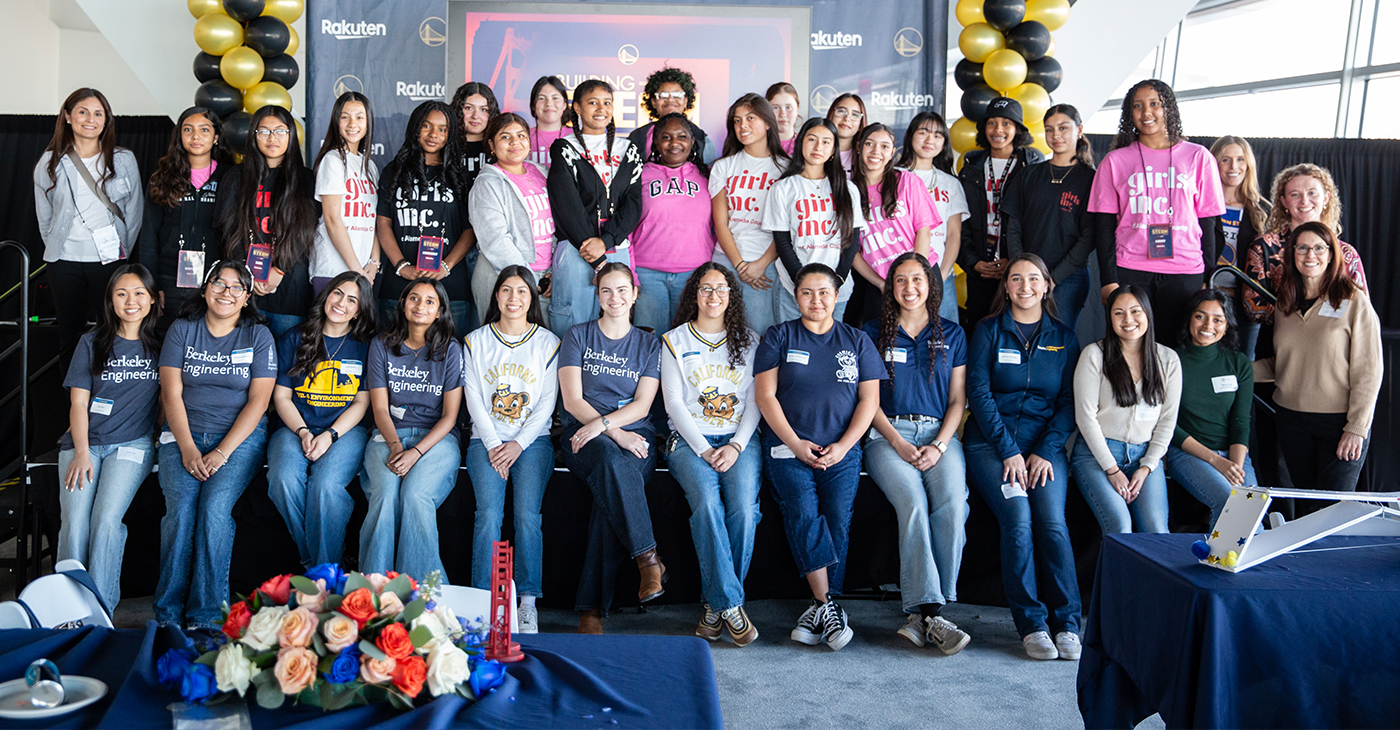
The Golden State Warriors and e-commerce giant Rakuten are joining forces to inspire the next generation of female engineers through Building STEAM Futures, part of The City Calls campaign.
Organizers say the initiative is founded on the idea that science, technology, engineering, arts, and mathematics (STEAM) are crucial fields for innovation and progress, and empowering young girls to pursue careers in these areas is more important than ever. Studies consistently show that girls are underrepresented in STEAM fields, resulting in a gender disparity that limits potential and hinders diversity.
Breaking down barriers and biases that deter young girls from pursuing STEAM subjects is essential for creating a level playing field and ensuring equal opportunities for all. By challenging stereotypes and promoting a culture of inclusivity and diversity in STEAM fields, experts believe young girls can be empowered to pursue their interests and aspirations without limitations confidently. Encouraging mentorship, providing access to resources, and celebrating girls’ achievements in STEAM are all crucial steps in creating a supportive environment that fosters success.
On Saturday, March 8, International Women’s Day, the Warriors and Rakuten hosted 20 middle school girls from Girls Inc. of Alameda County at Chase Center’s Above the Rim for a hands-on bridge-building experience. The young girls from Girls, Inc. of Alameda County had an opportunity to design, build and test their own bridge prototypes and learn the fundamentals of bridge construction from the Engineering Alliance and the UC Berkeley Steel Bridge Team.
This STEAM experience for the girls followed the first session in January, where they took a behind-the-scenes tour of the Golden Gate Bridge, learning about its design and construction from industry experts. The City Calls campaign, tipped off with the unveiling the Warriors’ new bridge-themed City Edition jerseys and court design earlier this year.
-

 Activism4 weeks ago
Desmond Gumbs — Visionary Founder, Mentor, and Builder of Opportunity
-

 Activism4 weeks ago
Families Across the U.S. Are Facing an ‘Affordability Crisis,’ Says United Way Bay Area
-

 Alameda County4 weeks ago
Oakland Council Expands Citywide Security Cameras Despite Major Opposition
-

 Alameda County4 weeks ago
Bling It On: Holiday Lights Brighten Dark Nights All Around the Bay
-

 Activism4 weeks ago
Black Arts Movement Business District Named New Cultural District in California
-
 Activism4 weeks ago
Lu Lu’s House is Not Just Toying Around with the Community
-

 Activism4 weeks ago
Oakland Post: Week of December 17 – 23, 2025
-

 Black History3 weeks ago
Alfred Cralle: Inventor of the Ice Cream Scoop

